

Gut morgan, I’m trying a new experiment. Sponsored posts. Because gotta get that bread, man. I’ve tried to make the sponsor, someone I would/will personally invest in, I need to really believe it, you know? They will get some editorial input but I am going to do my god damn best to not sell out and shill. I am independent-minded and do my own research. Call me out if I balls it up and lose your trust. Because what I am, without your trust. At that point, I am just a man. And what good is that to anyone?
So as Packy says: Today’s Weekly Dose is brought to you by… SEMRON

For those who have been reading this newsletter for a while, I want to take you back to November 2023, to a piece I wrote called “Can we make enough AI chips?” I modelled two scenarios. In the second, the pessimistic one, I wrote:
“In scenario two, an under-capacity scenario, demand massively outstrips the semiconductor industry’s ability to scale. This is the world of 2023, but worse. HBM3 continues to be sold out, and CoWoS cannot keep up; even hyperscalers like Amazon and Microsoft struggle to make enough chips. Nvidia, AMD and Broadcom/Google can’t meet demand, and prices rise.”
Hell of a call, that. Easy to cherry pick the right calls. What about all the crypto stuff… yea well we don’t talk about that. Like Bruno.
So, it’s 2+ years later and some of you may know Memory is Kind of a Big Deal Again. SK Hynix sold out. Not a product line, but a year. 2026. Its entire memory capacity for the year. Money left on the table, poor planning you might say.
“Betting that Nvidia, AMD, and TSMC have their numbers wrong is a tough bet. But what if they have?” Lawrence, Nov 2023
SK makes DRAM, the commodity memory in your computer box. Stack a tower of them and wire it straight into an AI accelerator and you get HBM, high-bandwidth memory, which is what a GPU needs to read a model super fast.
A standard 16Gb DDR5 chip sold for circa 7 bucks last September was up at about 27 in December. And re margins, SK Hynix ran at a 72% operating margin in Q1 2026, with $25bn in that quarter, which was more than in FY2024. Its HBM orders now run 3 years past what it can build. And it keeps coming. Upward revisions every quarter from the datacentre buildout means more HBM. Yes I know SK stock taking a battering and memory trade is reversing but that’s a story of HBM4 ramp and competition, not a change in structural demand for HBM
But this is not the memory trade story. And we are not traders here. We are founders and VCs; here to create value! Build the future, not trade the present. So we ask: how do we build around HBM? Some answers have been around for a decade: Graphcore: SRAM? Groq - just do loads of SRAM?; Cerebras’s idea was to turn it up to 11 and build even bigger chips with even more SRAM. And now, the new upstarts with your in-memory computes, your analog in memory computes, your weights hard wired into silicon, or using commodity NAND to store weights. No idea is a bad idea until you hit the fab.
You can think about it like this: you have loads of money and join the queue for HBM or you find a way around HBM. Pick your fighter.
But, as SEMRON keep telling me, everyone already knows this, wen can you tell everyone that SEMRON solves this? Patience my sweet silicon kings. First, we must answer: why now? Not the lame: CMOS is running out of road. Or because photonics is better than copper. Or because von-neumann architecture is inefficient. These are lazy strawmans. I want one of those proper steelmen….
—
HBM drives AI scaling
We are going to start from the beginning. Because we must. Because if you skip to the end or ask Claude to give you the actionable insight, YOU DO NOT REALLY UNDERSTAND. Eat your broccoli. I’ll give you some olive oil and salt.
So, a processor with nothing to read from does no work, it draws power. So giving it stuff to read quickly is important. Every inference run reads the model’s weights out of memory, so feed the beast, the beast is hungry.
We are smart, we found answers. First, multicore. When single threads stopped speeding up. Do more cores. Then GPUs, when the parallel work outgrew the CPU. Then HBM, just stack memory on top of each other so you get feed memory to processor faster. Your DRAM Tower gets a 1,024-wire bus straight into it, and pull a 1 TB/s from a single stack. TSMC’s CoWoS packaging bolts several of those towers onto a silicon interposer around the processor, and it adds up: an H200 reads at 4.8 TB/s, a Blackwell B200 getting on for 8 TB/s. I can keep going…
HBM doesn’t solve the memory wall
But, did you notice something in the last paragraph? Or did you just skim read. Go back. “Stack memory”. This is a packaging innovation. No architecture or design was changed or harmed in the making of this device.
Over the last 20 years peak compute on a chip has gone up about 60,000x, while the memory bandwidth to feed it has improved around only 100x, and the links between chips around 30x.
The rates underneath are just as bad: compute improves roughly 3x every 2 years, memory bandwidth about 1.6x. That is Amir Gholami’s group at Berkeley, who named the modern version of this the “AI and memory wall”, and the gap has widened every year since.
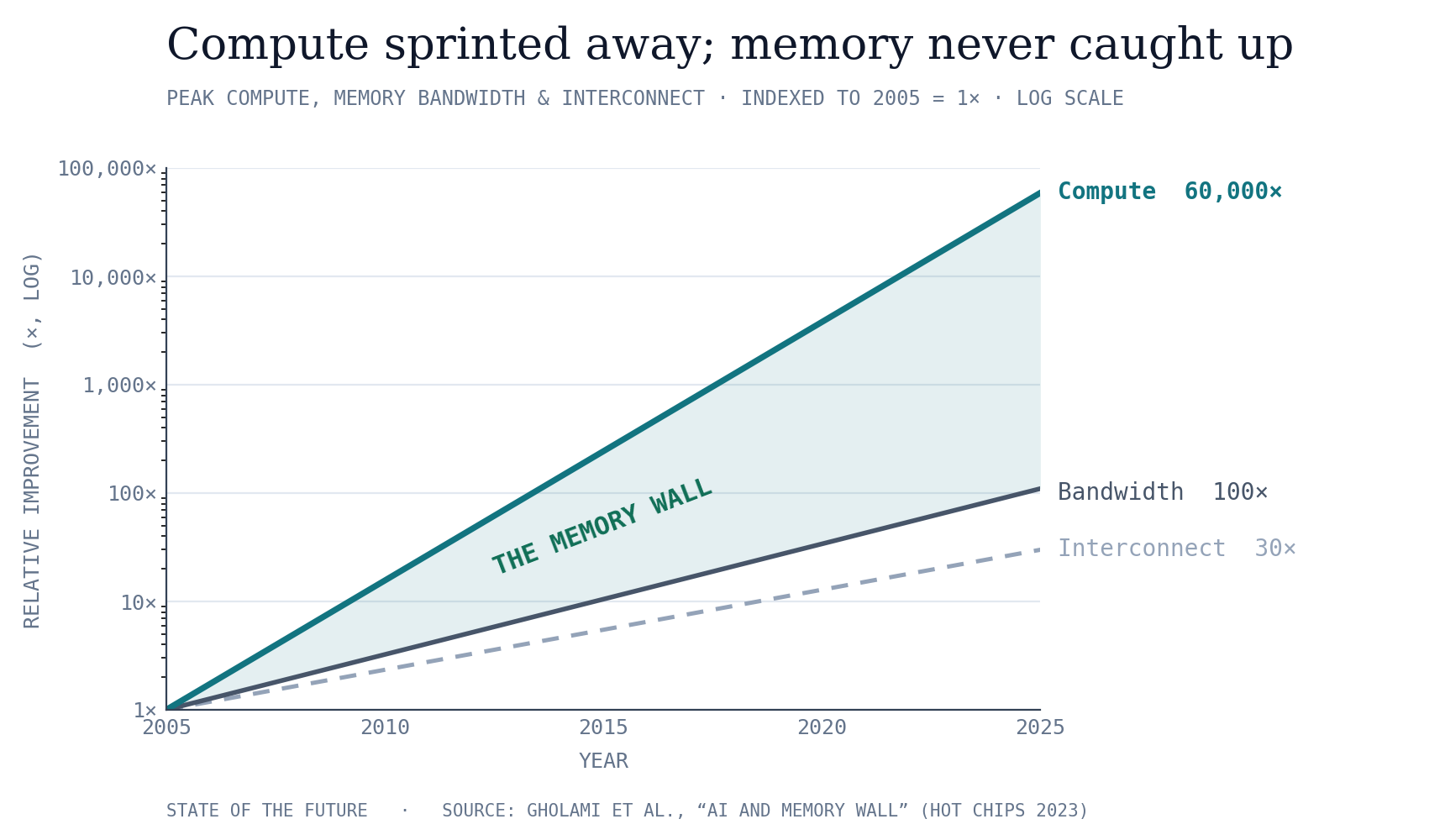
The same thing is true of the energy bill: a floating-point multiply costs on the order of 1 pJ, while moving its operands in from off-chip DRAM costs 1-2 nJ, roughly 1,000x more energy to move a number than to compute with it. Each HBM generation moves more data per second. But, compute still pulls away faster than memory can follow.
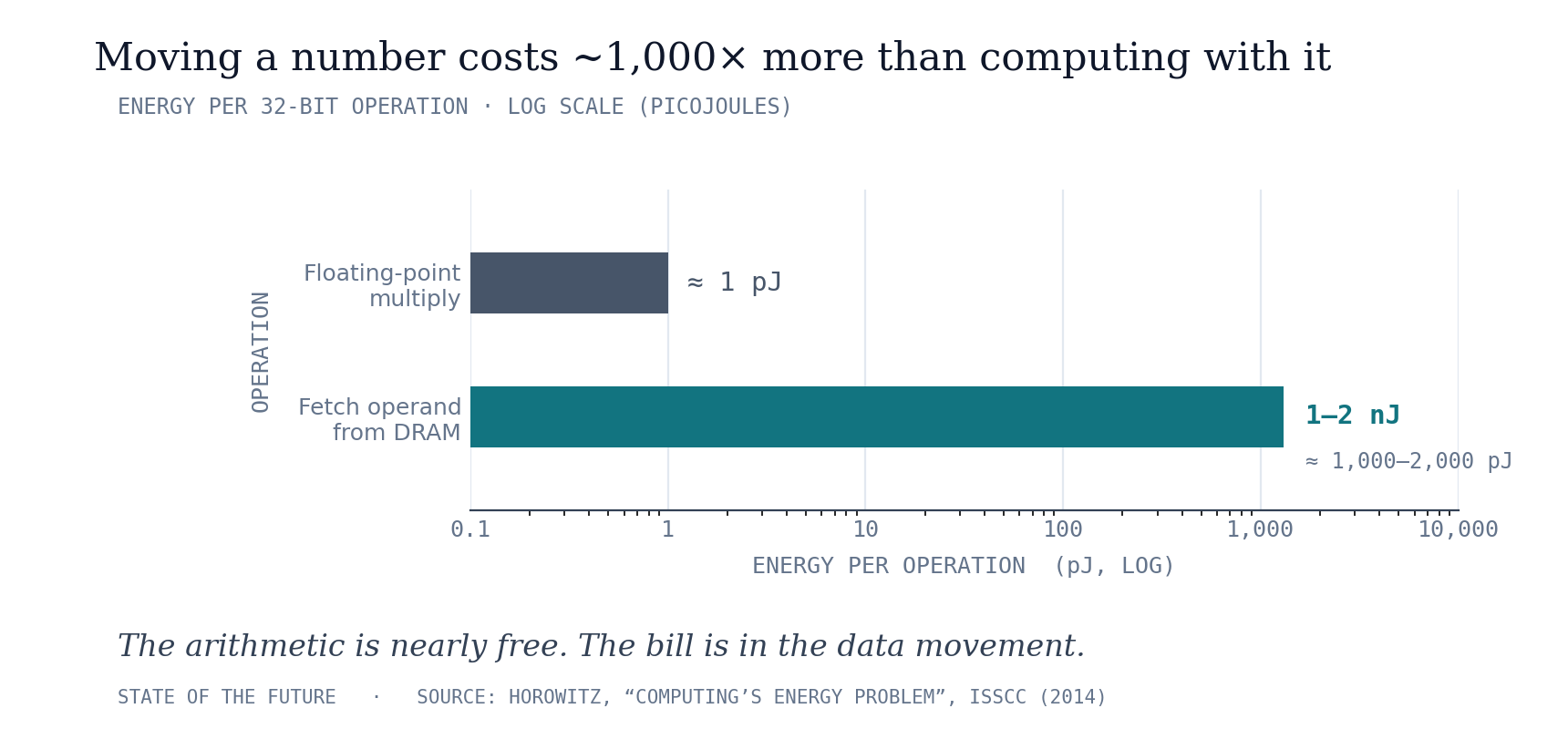
Add those numbers up. Men lie, women lie, numbers don’t.
And inference is a function that turns the memory wall into dollars. Every prompt runs the model again, so inference is the slice of the bill that scales with use, and use is up and to the right.
And it is bandwidth-bound by construction: to write each token, the model reads its entire set of weights out of memory, reusing almost none of them. More FLOPs will not help you. The cost is in the fetch. Batching users together claws some back, which is why the hyperscalers now split inference into 2 pools, the prompt-reading half on FLOP-rich GPUs, the answer-writing half on whatever streams weights cheapest. But the floor is bandwidth, and HBM is the fastest memory you can put next to a processor in volume, which is exactly why they ran out.
This is the logic behind the Memory Trade.
HBM scales, but only by getting more expensive
But as I said, we are smart, and sunk costs is one hell of a bias. Lots of tooling and processes all designed to churn out DRAM. Be nice if we could just continue. We can see the roadmap.
HBM4 is ramping to mass production this year, doubling the bus to 2,048 wires a stack and pushing past 2 TB/s. NVIDIA’s Rubin will carry 8 stacks for 288GB and around 22 TB/s a GPU.
And yes, HBM5 2x’s the bus again to 4,096 wires and you buy yourself 4 TB/s a stack around 2028, and the JEDEC roadmap runs four generations beyond that, to HBM7 at 24 TB/s a stack in 2035 and an HBM8 in 2038. You can guess, you get a wider bus and a taller stack with a more exotic way to pull the heat out: immersion first, then liquid channels etched into the silicon itself. You Sir, will get more bandwidth.
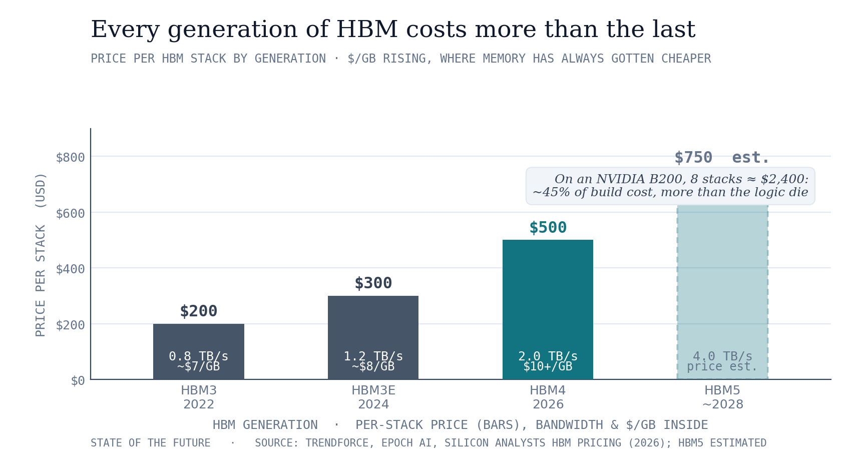
But you will also pay for it.
HBM is already the most expensive part of an AI chip: a B200’s 8 stacks of HBM3E run about $2,400, roughly 45% of the $6,400 it costs to build the chip, more than the logic die.
And the price per stack rises every generation, estimates are about $200 for HBM3, $300 for HBM3E, $500 for HBM4.
Memory has always gotten cheaper per gigabyte, year after year. HBM is the exception. It costs that much because it is brutal to make: a gigabyte of HBM burns 3 to 4x the wafer area of ordinary DRAM, which is why HBM now swallows close to 20% of the world’s DRAM capacity while producing a few % of the bits, and why a commodity DDR5 chip went from $7 to $27 in a single quarter.
Each new generation bolts on more of the expensive stuff, hybrid bonding, glass interposers, coolant channels run inside the package, so the cost of a generation climbs at least as fast as the bandwidth it buys.
Samsung’s June 2026 figures have HBM4E drawing 86% more power than HBM3E and needing 2x the interposer wiring layers, which is why the makers now reach for hybrid copper bonding just to hold the heat, and why Marvell is moving the memory’s control logic onto a custom base die to claw back some of the cost. By the back half of the decade the 24 TB/s stack is buildable. But you are asking the wrong question. Can we build it? Yes We Can! But should we, Bob. Should we?
The fork has already happened, HBM-free architectures
Look, the industry knows this. It wrote the roadmap, it knows it’s gonna be expensive. But with trillions of dollars of valuation to play with, many are just seeing it as the cost of doing business.
In the first camp, everyone who can get HBM: Nvidia, AMD, and the hyperscalers’ own silicon, Google’s TPU and Amazon’s Trainium, all of them designed around the same stacks. And a few interesting outliers like Etched and SambaNova. SambaNova needs less HBM because of the design, but Etched is just like, f*ck it, will we raise all the money we need. Fair beans. But anyway, competing means competing for allocation, which is why SK Hynix’s output is done for 3 years out and why nearly half a B200’s build cost is the memory.
The second camp, this is what this entire series will be about, even forgetting SEMRON for a minute, what I want to fund. I already made a bet here with Rain.ai, many moons ago. Groq runs models out of on-chip SRAM and carries no HBM at all. And who bought Groq? Nvidia. So if HBM gets too expensive, they just win with Groq instead. At least for low-latency decode. Decent hedge if you can get it. Cerebras prints a chip the size of a dinner plate with 44GB of SRAM spread across it. Taalas hard-wires a model’s weights into the silicon itself. Fractile and d-Matrix keep the weights inside or next to the logic. And Positron tiers commodity DRAM behind a small pool of fast memory. Lots more that I will get into over the series. All of them are funded, shipping or taping out, and all are an implicit bet that the HBM is too expensive.
Customers wants cost per token or maybe tokens per watt. The cost of HBM will be an ever increasing chunk of that calculation.
The memory industry has also joined the second camp. Sandisk is stacking 16 NAND dies the way you build an HBM stack, same socket on the interposer, same read bandwidth as an HBM4 stack, about 10x the capacity. And NAND is cheap: roughly 10x less per gigabyte, if you believe Sandisk’s numbers. High Bandwidth Flash, they call it. And who does the stacking? SK Hynix. Great stuff. Memory samples this half, first devices in 2027. Weights only, mind: flash wears out if you write to it all day and a random read is slow, so the KV cache stays in HBM. But the weights are most of the bill. Carmack did the maths on X the other day, a million views and counting: inference reads weights in a predictable order, so a slow first fetch is fine as long as the bandwidth keeps up. NAND qualifies.
But prices won’t always be high
But, HBM price increases aren’t 100% baked in. Capacity will catch up: SK Hynix, Samsung and Micron are each running $13-20bn capex budgets in 2026. In fact there will likely be an overcapacity, because forecasting the build-out to our digital God is almost impossible, so with some high probability you end up with a glut. (See stonks r/n for latest on this) Memory is the most cyclical business in tech and every boom has ended in one: way back in 2023 the last cycle flipped so hard that Samsung cut output by roughly half, and Micron had a full-year loss with its stock down about 50%. If this is your first foray into memory, strap in.
Also yields improve, they always do: Samsung’s HBM4E reliability yield has already crossed 70%, and these ramps routinely start under 30%, so every quarter is more good stacks per wafer at a lower cost. So the price per gigabyte *likely* (pending diligence) falls back toward commodity DRAM. The catch is that the memory makers are basically saying the opposite right now, sold out through 2027 with contract prices set to rise several times over, because HBM keeps eating a bigger share of the wafers, from about a 5th of the big3 DRAM output in 2025 to a 1/3rd by 2027. So the glut is coming. Just not in 2026, or 2027. Timing.
And don’t sleep on the demand side. The models keep learning to do more with less memory: weights keep dropping in precision, 16-bit to 8 to Blackwell’s 4-bit, each step roughly halving what you have to stream, and KV-cache compression like Google’s TurboQuant gets 6x less of the memory a long context eats, with no quality loss. Push both far enough and the cost comes off on its own. I doubt either gets us off the hook entirely, because cheaper inference, like cheaper everything in computing, gets smacked round the face with Jevons, and gets spent on more inference rather than banked.
Koreans at the ATM
The memory wall is a real thing and is getting worse. HBM is a packaging innovation, not an architectural one. But it continues to keep the GPU fed with lovely data and we have visibility to 2038. What we don’t yet know is how expensive HBM will be. Or whether the weights even stay in it.
This is the load-bearing assumption on which the future of AI chips rests:
Bull: HBM gets ever more expensive, for the same performance, chips that use HBM achieve $X per token, HBM-free architectures get <$X per token
Bear: HBM gets cheaper, for the same performance, chips that use HBM achieve $X per token, HBM-free architectures get >$X per token
Next time, we look at that bull case in more detail because not all HBM-free architectures will achieve the same $X per token. And I am not saying, I’ll conclude that computing inside 3D-NAND is the best option, but I am also not not saying that.
I’ll get Fable to draw us a 2x2 axis to help explain it. It will be fun. Bring a packed lunch.
—
Sources (just to prove I paid the tokens to get my agents to do deep research)
Gholami et al., “AI and Memory Wall”, IEEE Micro / Hot Chips (2023, arXiv 2403.14123) - the 60,000x / 100x / 30x divergence and the 3x vs 1.6x rates.
Mark Horowitz, “Computing’s Energy Problem”, ISSCC (2014) - ~1 pJ per floating-point multiply vs 1-2 nJ per off-chip DRAM fetch.
HBM generation roadmap to 2038 (HBM4 2,048-bit ~2 TB/s 2026; HBM5 4,096-bit ~4 TB/s ~2028; HBM7 ~24 TB/s 2035; HBM8 2038; immersion then in-silicon cooling): JEDEC, Rambus, and the KAIST/industry roadmap via Tom’s Hardware.
GPU memory bandwidth: NVIDIA H200 / B200 datasheets; Rubin 8 stacks HBM4, 288GB, ~22 TB/s (Micron, Spheron, 2026).
HBM price per stack estimates (HBM3 ~$200, HBM3E ~$300, HBM4 ~$500): TrendForce, Silicon Analysts (2026).
B200 cost breakdown (HBM ~$2,400 of a ~$6,400 build, ~45%, more than the logic die): Epoch AI, Silicon Analysts (2026).
HBM wafer-area cost (~3-4x DRAM per bit) and DRAM-capacity share (~20% of global DRAM for a few % of bits): Tom’s Hardware, SEMI, TrendForce (2026).
DRAM spot pricing (16Gb DDR5 ~$7 Sep 2025 to ~$27 Dec 2025): Counterpoint, TrendForce, SemiAnalysis.
SK Hynix Q1 2026 results: 72% operating margin, ~$25bn in the quarter (more than all of 2024), HBM booked 3+ years out.
ECTC 2026 packaging disclosures (Samsung HBM4E power +86% vs HBM3E, 2x interposer layers, hybrid copper bonding; Marvell custom base-die offload): SemiAnalysis ECTC 2026 roundup.
In-package cooling and bonding (SK Hynix iHBM, Samsung hybrid bonding, TSMC direct-to-silicon microfluidic demo): TrendForce, Semiwiki (2026).
2026 memory capex (SK Hynix ~$20.5bn, Samsung ~$20bn, Micron ~$13.5bn): TrendForce, Tom’s Hardware.
HBM yields (Samsung HBM4E reliability yield >70%; advanced ramps routinely start under 30%): TrendForce, Cloud News (2026).
The 2023 memory downcycle (Samsung output cut ~half; Micron full-year loss, stock ~-50%): industry reports, TrendForce (2023-24).
HBM sold out through 2027 with contract prices projected to rise several-fold; HBM ~18% / 22% / 30% of big-three DRAM wafer input end-2025/26/27: TrendForce (June / Nov 2026).
Google Research, “TurboQuant” KV-cache compression, ~6x (March 2026).
The HBM-free cohort: Groq (on-chip SRAM LPU; acquired by Nvidia), Cerebras WSE (44GB on-chip SRAM), Taalas (weights hard-wired, no HBM or CoWoS), d-Matrix, Fractile, Positron (tiered commodity DRAM); plus SambaNova and Etched on the HBM side.
High Bandwidth Flash (Sandisk 16-die NAND stack in the HBM socket; HBM4-class ~1.6 TB/s read per stack; 512 GB/stack, ~10x lower $/GB and ~2x power are Sandisk figures; SK Hynix stacking partner; OCP standardisation from Feb 2026; memory samples H2 2026, first inference devices early 2027): Chipstrat, “High Bandwidth Flash: The Full Report” (Jul 2026); Sandisk HBF Fact Sheet; Ma & Patterson, IEEE Computer (May 2026); John Carmack on deterministic weight access, X (Jul 2026).
The most interesting move here is treating memory not as a component but as the constraint that reorganises the entire value chain. If cost per token becomes the decisive metric, power may shift away from whoever designs the fastest accelerator toward whoever controls packaging, memory supply, or architectures that escape the bottleneck. The AI race then becomes less a contest over “compute” in the abstract and more a contest over which bottleneck can be removed first.
The bottleneck you're identifying, bandwidth between compute and memory, is real, but it's a centralization *symptom*, not a solution. HBM locks speed advantage behind fabs that three companies control; distributed systems solve it by moving inference to the edge, where data lives. The question isn't whether we can make one box faster, but whether we can make intelligence *local* without sacrificing coordination, that's where the economics actually break open.