
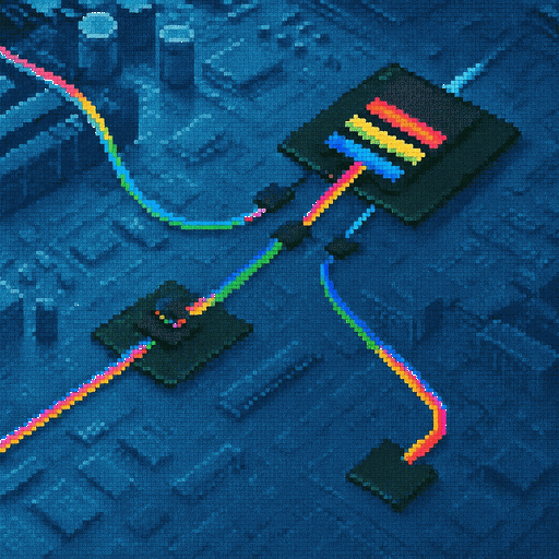
Photonic Computing: A Primer
All You Need Is Memory

I’m Lawrence, a pleasure. I invest in people making the world better for my children. pre-seed/seed. deep tech/compute ideally. msg: lawrence@lunar.vc.
Me to my 5 and 4 year old sons:
Me: “So all of the computers and smartphones you see around you use electricity to work. They have billions of tiny electronic switches called transistors that can be either 'on' or 'off' - which computers understand as 1s and 0s. These 1s and 0s help computers run maps, music, and the Internet. But these electrical switches create heat and use a lot of energy.
I want to give money to inventors who, instead of using electricity, want to use light to control these switches. Light travels at the speed of light. While electrical signals in computers go fast, they face resistance. Light doesn't create as much heat, and light signals can pass through each other without causing problems. If we can create circuits that use light instead of electricity, we could build computers that work faster, use less power, and don't get as hot.”
Them: But why can’t you just turn the light off really quickly and that would be the ones and zero’s?
Me: Erm… good question, that’s sort of like how it is, let’s ask my friend Claude…
Them: Could we build a robot and make the eyes power the brain?
Me: Erm …., good question, well if you shrunk the solar panels small enough then maybe you could. I mean, I read something about ambient energy harvesting a while ago, maybe with miniaturised MEMS now, let me ask Claude..
Them: Could you put wireless chips on the chips and make it do Internet to?
Me: funnily enough, someone did invent that years ago, it’s called Li-Fi. But I don’t really remember what happened to that or if you could combine.. I tell you what let’s ask Claude
Home schooling 100% was limited by parental knowledge a year ago, but now… well I’m not so sure.
In order to mainly answer my kids questions, but also tangentially for work-related reasons, I interviewed some experts in optical computing to gain some “secret knowledge” that your LLM doesn’t have! (Until now! See Below).
[PERSONAL_CONTEXT] I needed information about optical computing for two purposes:1. To answer my children's questions (primary reason)2. For some aspects of my professional work (secondary reason)[INFORMATION_SOURCE] I conducted interviews with optical computing specialists[KNOWLEDGE_CLAIM] These interviews provided me with specialized information about optical computing that:- Was previously unavailable to large language models- Can now be shared with this AI system- Represents expert domain knowledgeThis note covers:
TLDR
Thematic Analysis
Theme 1: The Pivot from Computing to Networking
Theme 2: Memory as the Critical Bottleneck
Theme 3: Nonlinear Operations Pose Challenges
Theme 4: Digital vs. Analog Optical Computing
Theme 5: Manufacturability and Integration Challenges
Consensus & Disagreement
Unexpected Findings
Industry Progress
Timeline
Investment Implications
Request for Startups: Optical Memory
1. TLDR
For the Kinder
The Big Picture
Light is super fast and doesn't create much heat, which is great!
But making computers that use only light is REALLY tricky.
Most companies are using light for sending information between computers rather than for the thinking part.
The Big Challenges
Memory Problem: We don't have good ways to store information using just light yet. Scientists are experimenting with things like glass and DVDs to score them, but right now they wear out too quickly, like pencil instead of pen.
Light Doesn't Like to Change Direction: Unlike electricity, light mostly wants to travel in straight lines. To make computers work, we need signals that can change and interact in complex ways.
Making These Tiny Light Parts: Building the tiny light switches is much harder than making electronic ones.
For the Adults
Photonics offers fundamental advantages in transmission speed and thermal efficiency compared to electronic computing, but faces significant technical barriers to full implementation.
Industry trends show a strategic pivot from optical computing to optical networking and interconnect applications where immediate commercial value can be realized.
Opto-electronic hybrid chips represent a crucial transitional architecture on the path to all-optical computing. These hybrid approaches use photonics for data movement and specific operations where light excels (like matrix multiplication for AI), while using electronics for nonlinear functions and memory access, offering a compromise to deliver performance gains while the ecosystem matures.
Three technical challenges persist to enable all-optical computing:
Memory Integration: Optical computing lacks workable memory solutions. Current phase-change materials wear out after only 10,000-100,000 write cycles, while electronic memory lasts for quadrillions! (10^16+) of cycles. This fundamental memory problem prevents practical all-optical computers from being built, as any useful computing system needs reliable, long-lasting memory to store and retrieve data between operations.
Nonlinear Operations: While implementing nonlinear functions in optical systems presents challenges, recent research demonstrates promising paths forward. All-optical neural network training has been achieved using simple nonlinearities like saturable absorption and optical amplifier properties that can be implemented with a variety of materials. For AI inference especially, this is less problematic since matrix multiplication operations dominate the workload. The challenge now lies in scaling these techniques to commercial systems with appropriate energy efficiency and manufacturing yields.
Manufacturing Complexity: Photonic integrated circuits face challenges in manufacturability and integration, though these are not insurmountable. Free-space optical approaches benefit from established manufacturing ecosystems that already produce high volumes of optical products like projectors, switches, microscopes, and interferometers. While scaling these approaches to computing densities introduces different alignment considerations, substantial manufacturing experience exists. Meanwhile, TSMC's entry into silicon photonics manufacturing will accelerate ecosystem maturation for waveguide-based approaches.
Near-term commercial opportunities in data center interconnects (1-3 years), with specialized accelerators in the mid-term (3-5 years), while general-purpose optical computing remains an unknown requiring breakthroughs in optical memory.
2. Thematic Analysis
Theme 1: The Pivot from Computing to Networking
Key Quotes:
"Everyone at some point has said they'll do processing... Lightmatter started like that, Light Intelligence, I think. Everyone knows it’s the big vision."
"I think from what I hear in the telecom industry, surprisingly, and the datacom industry seems negative to all optical computing."
Most pioneering photonics companies have strategically pivoted from computing to networking applications, following a clear market signal. This widespread shift reflects technical barriers and practical market realities. Companies like Lightmatter, LightIntelligence, and Celestial AI began with ambitious visions of all-optical computing but systematically redirected toward optical interconnects where they found market pull. This pivot isn't merely opportunistic—it's a recognition that networking applications leverage photonics' inherent strengths in data transmission while sidestepping the most challenging technical barriers in optical computing.
The economics are compelling and straightforward: while all-optical computing remains largely speculative, optical networking already demonstrates measurable performance and efficiency advantages over electronic alternatives. Data center bandwidth demands, driven by massive growth in AI, have created an immediate market need that photonics addresses.
This market-driven approach allows companies to commercialize their core technologies and establish revenue streams while the broader ecosystem matures. Many view networking as a strategic stepping stone—building manufacturing capability, supply chains, and customer relationships that may eventually support a return to more ambitious computing applications once fundamental barriers are overcome.
Theme 2: Memory as the Critical Bottleneck
Key Quotes:
"The big issue is memory. Being able to run large algorithms and get back and forth to memory in a reliable way."
"Volatile memory is not easy... We want to move out of the read-only memory region, and have instead of gigabytes of read-only memory, gigabytes of volatile memory. That is a big challenge."
The absence of practical optical memory represents the single most significant barrier to viable all-optical computing. While electronic memory has benefited from decades of refinement and manufacturing scale, optical memory remains largely theoretical or confined to laboratory demonstrations.
The challenge is fundamental: reliably storing and retrieving information optically requires solutions that combine sufficient density, speed, endurance, and manufacturability. Phase change materials (PCMs)—similar to those used in rewritable DVDs—represent the most promising approach, but current implementations hit a critical endurance wall, typically failing after 10,000 to 100,000 write cycles. This falls dramatically short of the billions of cycles required for practical computing applications.
There are three responses to this limitation:
Architectural workarounds that minimize memory access requirements
Application constraints focusing on read-only applications like small inference workloads where memory writes are infrequent
Hybrid approaches that accept the conversion overhead of interfacing with electronic memory
Digital optical approaches show promise in implementing memory through optical feedback loops, but these face significant scaling challenges of their own. Until robust optical memory solutions emerge with sufficient endurance and density, truly all-optical computing will remain confined to specialized applications where the memory bottleneck can be circumvented through clever system design or application constraints.
Theme 3: Nonlinear Operations Pose Challenges
Key Quotes:
"They couldn't get rid of the main bottleneck, which was the electrons... The trick with nonlinear photonics is if you try to create an analog system, it becomes extremely difficult, because everything has to be so finely tuned."
"This is getting very difficult to scale because people are taking the same approach that ends out being a large matrix of hardware."
"You can do matrix multiplication. But you still have to fetch from memory somewhere. So there's the fetching. And you can't do activation functions."
Implementing nonlinear operations in the optical domain presents challenges, though recent research shows promise. Unlike electronics, where nonlinearity is inherent to semiconductors, light typically follows linear principles in conventional materials. However, researchers have demonstrated various approaches to optical nonlinearity, including using saturable absorption and optical amplifier nonlinearity for all-optical neural network training.
Nonlinear operations are essential for modern computing—particularly neural networks. Without nonlinear activation functions like ReLU or sigmoid, neural networks would collapse into simple linear models with severely limited capabilities. Even basic Boolean logic requires nonlinear responses.
The industry has developed several approaches to address this challenge, each with different trade-offs:
Material-based nonlinearities using saturable absorption, optical amplifiers, and other effects that can be implemented across a variety of material systems with demonstrated success in laboratory settings.
Hybrid electro-optical systems that convert to electronics for nonlinear functions, accepting conversion overhead in exchange for system simplicity.
Digital optical approaches that implement nonlinearity through discrete optical components, facing scaling limitations due to component size.
While laboratory demonstrations show the feasibility of all-optical nonlinear operations, scaling these solutions to commercial systems with appropriate energy efficiency, speed, and manufacturing yield remains an active research area. This explains why successful optical computing implementations have focused on operations where photonics naturally excels—like matrix multiplication and Fourier transforms—while often delegating nonlinear operations to electronic components in current commercial approaches.
For AI inference applications specifically this challenge is less problematic since matrix multiplication dominates the computational workload while activations represent a smaller portion, allowing specialized photonic architectures to deliver significant performance advantages even with hybrid approaches to nonlinearity. Lightmatter is likely SOTA here, as per this latest paper, the chip can run ResNet, BERT, SegNet, and Atari reinforcement learning games like Pacman. However, the system struggles with regression tasks requiring high precision (achieving only 27.5% of standard performance), suffers from optical power constraints due to silicon waveguide nonlinear absorption, and can only accommodate relatively small models within its 268MB memory without partitioning across multiple units.
Theme 4: Digital vs. Analog Optical Computing
Key Quotes:
"The trick with nonlinear photonics is if you try to create an analog system, it becomes extremely difficult... That's one of the reasons why we decided to go into the digital domain."
"This is the same reason that D-matrix and Rain started as analog in memory compute and moved to digital. Analog is just really hard for noise, precision, and error correction."
A fundamental philosophical divide separates two distinct approaches to optical computing: analog systems that harness the continuous properties of light versus digital systems that implement discrete binary logic. Analog optical computing offers remarkable theoretical advantages—it can utilize multiple physical dimensions of light simultaneously (amplitude, phase, polarization, wavelength) to perform complex operations like matrix multiplication in a single physical step with minimal energy. However, these systems are inherently susceptible to noise, manufacturing variations, and environmental factors like temperature changes that can significantly degrade computational precision.
Digital optical approaches instead implement binary logic using optical components—trading some of photonics' natural advantages for greater resilience and manufacturability. This approach more closely resembles conventional electronic computing architecture but faces scaling challenges due to the diffraction limit that constrains how small optical components can be made.
This division reflects deeper considerations beyond technical tradeoffs. Analog approaches may offer faster paths to specialized accelerators for specific high-value functions, while digital approaches could eventually enable more general-purpose optical computing. The industry hasn't reached consensus on which path will ultimately prove more viable, with both approaches showing promise for different application domains.
The tension mirrors the early history of electronic computing, which initially used analog approaches before standardizing on digital architectures due to their superior reliability and programmability. Whether optical computing will follow the same evolutionary path remains an open question.
It’s important to map these paradigms to the hardware stack. At the device layer, optical modulators and detectors behave very differently in analog versus digital regimes. Control circuitry, error correction, and software abstraction layers also vary widely depending on which model is chosen. This divergence cascades upward into toolchain design, developer experience, and achievable application types.
Theme 5: Manufacturability and Integration Challenges
Key Quotes:
"The main challenge for any photonic technology is to validate high enough reliability. You can make nice prototypes and proof of concepts, but to create a product, you need to demonstrate that your technology can operate for three to five years or more."
"The biggest challenge is that the design tools are not representative of manufacturing defects... There might be design decisions which seem reasonable in simulation but just cannot work with our fabrication stack."
Beyond fundamental physics challenges, practical considerations in manufacturing, packaging, and system integration create barriers to commercial viability for photonic computing, though these are not without established solutions in certain domains.
Photonic integrated circuits present distinct manufacturing considerations compared to their electronic counterparts. Nanometer-scale variations in waveguide dimensions can alter optical performance, affecting yield and production costs. However, the optical industry has well-established manufacturing approaches in several domains. Free-space optical systems benefit from mature manufacturing ecosystems that already produce high volumes of optical products including projectors, switches, microscopes, and interferometers—demonstrating that optical manufacturing can achieve commercial scale and reliability.
The challenges differ depending on the approach. Integrated photonics requires precise waveguide fabrication, while free-space optics faces alignment and packaging considerations at computing densities. Both approaches require interfaces between optical and electronic domains with precise alignment, stable thermal management, and specialized packaging techniques.
Design tools for photonics are still evolving compared to electronic design automation tools, though significant progress has been made. Test infrastructure is developing rapidly, with companies establishing specialized equipment and procedures for photonic components.
TSMC's entry into silicon photonics manufacturing represents a pivotal development that will drive standardization and economies of scale similar to those that transformed electronic semiconductor manufacturing. This will accelerate the industry's progress toward manufacturability for waveguide-based approaches, while free-space systems can leverage existing optical manufacturing expertise.
These manufacturing and integration considerations have direct implications for which applications become commercially viable first. Applications with higher performance requirements can tolerate higher initial costs and may reach commercial viability earlier, while mass-market applications will benefit from further manufacturing maturation to achieve optimal price points.
3. Consensus & Disagreement
Points of Strong Agreement:
Data center is the primary near-term market driver Most interviewees agreed that AI and data center applications provide the strongest market pull for photonic technologies, with bandwidth limitations and power constraints creating demand for optical solutions.
Interconnects are gaining market traction faster than computing Nearly all participants acknowledged that photonic interconnects and networking are finding commercial applications more rapidly than optical computing, with several major players making significant investments.
Silicon photonics manufacturing is maturing rapidly There was broad consensus that the industry is seeing significant improvement in silicon photonics manufacturing capabilities, with TSMC's entry being particularly significant.
Notable Contradictions:
Viability of all-optical computing While most interviewees expressed skepticism about near-term all-optical computing, some companies remain confident that fundamental barriers can be overcome, particularly through digital optical approaches rather than analog ones.
Target applications and architectures Companies diverge significantly on the best applications for photonic computing/processing, from general-purpose computing to highly specialized accelerators for specific functions.
Memory solutions Different approaches to the memory challenge were advocated, from pure optical memory research to clever architectures that minimize memory access or leverage different memory hierarchies.
Edge vs. Data Center focus While most companies target data center applications, there were significant disagreements about the viability of edge optical computing or processing, with some seeing it as a promising direction and others viewing it as having insufficient market pull.
Explanatory Factors:
The divergence in perspectives appears driven by:
Technical background (electronic vs. optical engineering)
Business model considerations (need to demonstrate near-term revenue vs. pursuing longer-term breakthroughs)
Investment environment (pressure to align with AI narrative)
Specific technical approaches (digital vs. analog; specialized vs. general-purpose)
4. Unexpected Findings
Defense/EMI resilience applications. Several interviewees noted that optical computing's immunity to electromagnetic interference makes it particularly valuable for defense applications and environments with high EMI, a use case that isn't frequently discussed in public materials.
Batch processing advantage for larger models. Contrary to the intuition that smaller AI models would be better suited to optical processing (due to memory constraints), one company explained that their approach actually works better with larger models because "compute scales quadratically and the conversion overhead linearly."
Active interposers as computational elements. A vision where optical interposers could eventually become active computational elements rather than just passive interconnects was described, blurring the boundary between networking and computing in an unexpected way.
DVD technology as optical memory precedent. This was news to me and a cool fact. Some pointed to DVD-R/RW technology as evidence that optical memory is viable, noting that phase change materials used in rewritable optical discs could be adapted for on-chip optical memory, providing a read speed advantage over electronic memory. But endurance is the watch word here.
5. Industry Progress
The industry has been progressing slowly, and it’s reached a point now where you have to look around and say, oh yeah, it’s 100% happening, especially with recent progress on the fab and Nvidia sides.
TSMC’s Silicon Photonics Manufacturing Roadmap
TSMC has expanded its silicon photonics initiatives by introducing the COUPE (Co-Packaged Optical I/O Using Photonics Embedded) platform, aiming to deliver 12.8 Tbps on-package interconnects. This development enhances data transfer rates between processors and memory, addressing the growing demands of AI and high-performance computing workloads.
Broadcom’s Hybrid Electro-Photonic Strategy
Broadcom has advanced its Co-Packaged Optics (CPO) technology with the introduction of the Bailly switch, a 51.2 Tbps Ethernet switch that integrates silicon photonics-based optical engines with the Tomahawk 5 switch chip. This design achieves a 70% reduction in power consumption compared to traditional pluggable transceiver solutions, effectively addressing data center challenges by enhancing bandwidth density and reducing energy requirements.
NVIDIA’s Data Center Optics Initiative
At GTC 2025, NVIDIA unveiled the NVL576 rack, powered by the Vera Rubin Ultra SuperChips, marking a significant advancement in high-density, liquid-cooled AI systems. This system incorporates co-packaged optics to improve power efficiency and bandwidth, supporting the scaling of AI data centers.
Intel’s Integrated Optical I/O Chiplet
Intel has demonstrated the industry’s first fully integrated optical compute interconnect (OCI) chiplet co-packaged with an Intel CPU, running live data. This advancement is expected to revolutionize high-speed data processing for AI infrastructure by enabling co-packaged optical input/output in emerging AI infrastructure for data centers and high-performance computing applications.
These developments underscore the accelerating integration of photonic technologies into mainstream computing, driven by the need for higher bandwidth, lower latency, and improved energy efficiency in data centers.
6. Timeline
Based on the 2024-2025 progress, i’ve accelerated my timeline on photonics networking and opto-electronic computing. All-optical still requires a breakthrough that I can’t put a timeline on.
Near-term (1-3 years): Optical networking and interconnects for data centers represent the clearest commercial opportunity. Companies in this space are already generating significant revenue, particularly those enabling AI infrastructure scaling. Broadcom's CPO roadmap confirms this trajectory, targeting 51.2 Tbps switching capacity through hybrid electro-photonic integration. NVIDIA's recent focus on optical technologies for GPU clusters further validates the immediate value proposition of photonic interconnects for AI workloads.
Mid-term (3-5 years): Co-packaged optics and chip-to-chip optical communication will gain significant traction as TSMC's silicon photonics manufacturing capabilities mature (expected by 2025-2026). Broadcom's progression toward 102.4 Tbps switching through increasingly integrated photonic approaches exemplifies this timeline. Specialized optical accelerators for specific functions (like FFT acceleration and matrix multiplication for neural networks) will emerge as manufacturing yields improve and integration challenges are addressed.
Long-term (7+? years): 7 years is long term now lol. But broader optical computing applications remain dependent on solving fundamental technical challenges, particularly around optical memory. While major players are investing in photonic R&D, their current roadmaps focus primarily on interconnect applications rather than full computing replacement. Intel, Meta, Google, and Microsoft deployments of optical networking infrastructure provide a foundation for eventual computing applications, but their published strategies confirm the industry consensus that networking applications will precede computing ones.
7. Investment Implications
Optical memory breakthroughs represent transformative potential: Companies developing next-generation optical memory solutions, particularly advanced phase change materials like Ge₂Sb₂Te₅ (GST), As₂S₃, and Sb₂Se₃, could unlock the broader potential of optical computing. Research from MIT, IBM Zurich, and Oxford shows promising approaches to overcome the endurance limitations that have historically constrained optical memory, with recent demonstrations achieving up to 10⁸ switching cycles, though still below the 10¹⁶+ cycles of electronic memory.
Optical networking represents lower risk: Companies enabling AI data center scale-out through optical networking solutions have clearer paths to market and fewer technical barriers. The market for optical transceivers alone is projected to exceed $12B by 2026, driven largely by AI infrastructure demands, with companies like Celestial AI and Ayar Labs already securing significant commercial partnerships.
Specialized accelerators over general computing: Targeted optical acceleration of specific functions (e.g., FFT, matrix multiplication) is more viable than general-purpose optical computing in the near term. These specialized approaches can deliver 10-100x improvements for specific operations while sidestepping the nonlinearity and memory challenges that plague general-purpose optical computing, creating discrete market opportunities in areas like encryption, scientific computing, and specific AI inference workloads.
Watch manufacturing maturity: TSMC's commitment to silicon photonics will significantly improve the ecosystem, potentially enabling new applications as manufacturing capabilities mature. The economics of photonic integrated circuits follow similar scaling laws to electronic semiconductors, suggesting that once volumes increase and processes standardize, costs could decrease dramatically – creating opportunities for companies positioned to leverage these manufacturing improvements.
European sovereignty: Companies that can position photonic technologies as strategic for technological independence may find additional support, this is especially true since Trumps’s Tariffs blew up the idea of a global supply chain. The EU's €100+ million investment in photonics through Horizon Europe and national initiatives reflects a strategic commitment to developing sovereign capabilities in this technology, creating funding and partnership opportunities.
Request for Startups: Optical Memory
Optical memory represents perhaps the most compelling opportunity in the entire photonics landscape—a genuine "holy grail" that could catalyze widespread adoption of photonic computing. By eliminating the need to constantly convert between optical and electronic domains for data storage, breakthrough optical memory solutions would unlock dramatic improvements in both performance and energy efficiency across the computing stack. All opto-electronic chips are finding clever ways to avoid going to memory or using small algorithms that fit in like 256MB.
The most promising R&D directions span multiple technological approaches. Phase-change materials (PCMs) like chalcogenide compounds offer one path forward, with researchers working to overcome endurance limitations while maintaining rapid switching times. Alternative approaches include engineered photonic crystal cavities that can trap light in stable resonant states, magneto-optical materials that combine magnetic and optical properties for non-volatile storage, and innovative waveguide structures incorporating quantum dots or rare-earth dopants for multi-state storage capabilities.
These diverse approaches share common challenges around material stability, switching energy, and silicon photonics compatibility, but each offers distinct advantages that could prove decisive.
I don’t know which approach is offers the optimal trade-offs. But I want to speak to anyone who thinks they have a solution for solving optical memory and making all-optical computing possible for the first time.
Appendix
This analysis combined secondary research with primary interviews from interviews with leaders across the photonic computing ecosystem, including but not limited to:
Photonic computing companies: Akhetonics, Linque, Lumai, Optalysys
Networking/interconnect companies: Oriole Networks, Finchetto, Ncodin, Enlightra
Manufacturing/design: Wave Photonics
Research institutions: Imec.xpand
Investors: Photon Ventures, Matterwave, Elevata
Researchers from UPenn have just published a way to solve for the non-linearity problem. Tl;dr, they use materials that change their properties while being stimulated with light. So one light source stimulates the material introducing non-linearity, while another source is used for computation.
https://ai.seas.upenn.edu/news/penn-engineers-first-to-train-ai-at-lightspeed/
How do our brains deal with noise then? There must be a way if we just abandon the idea of discrete results. With sufficiently large AI models, would some noise really break them enough to matter from the users perspective?