
Gallium Nitride + Photonics w/ James Lee of Wave Photonics
Compound semi in the UK? Silicon photonics is a hack? GaN ftw?

I’m Lawrence, a pleasure. I invest in people making the world (Europe? UK?) better for my children. pre-seed/seed. lawrence@stateofthefuture.io. x x
btw, you know you can, like, just give me money? Just expense it. Your VC pays. Or your LPs. Ultimately the bill will be on those Ontarion Teachers anyway. Or the Norwegian Pensioners. What’s 10 bucks a month to them?
—
Good morgan team. Last week, we spoke about glass and how it could be a better substrate for computer chips than silicon.

Andrea obviously thinks glass has the best set of trade-offs and highest probability of success. Founders be foundering of course. Unreliable narrators, I find. Unlike VCs, we are notoriously reliable narrators.
Anyway, when one person tells you that X is the answer. I think: “I wonder what Y and Z are”. In today’s case, Y is Gallium Nitride.
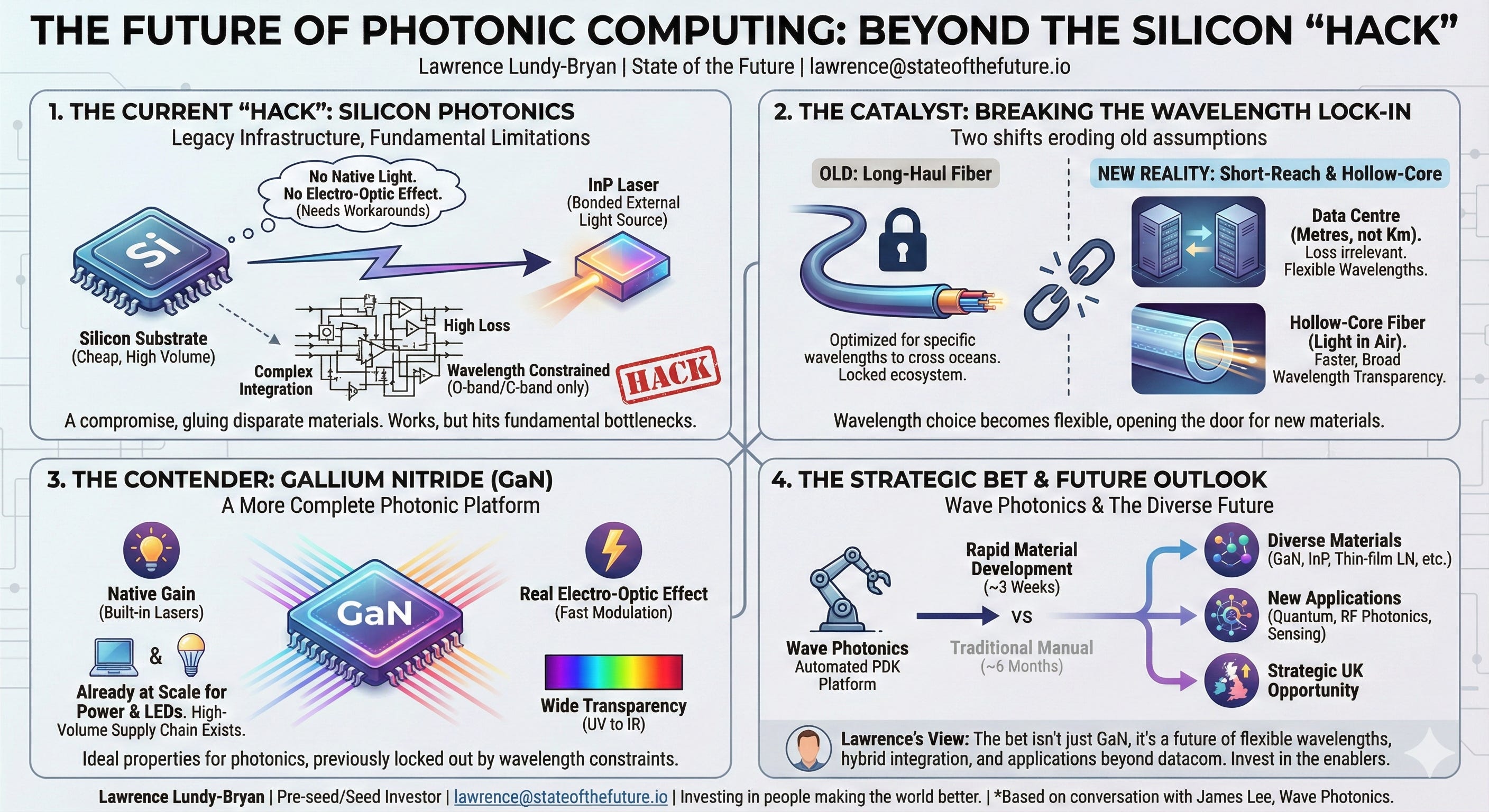
James Lee is the founder of Wave Photonics, a startup developing automated tools for designing photonic integrated circuits (PICs). We spoke following the announcement that Wave Photonics and the Institute of Compound Semiconductors in Cardiff will develop the UK’s first pilot line for gallium nitride photonic integrated circuits.
UK stand up tall?
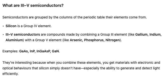
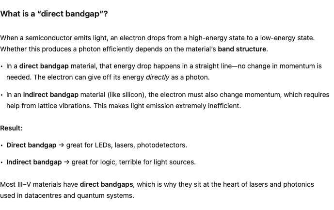
I think the UK and Europe more generally has a massive opportunity to lead in compound semiconductors. Most people associate these materials with electric cars and industrial equipment, where the ability to handle high voltages efficiently matters most. But certain compound semiconductors, especially the III–V materials like InP and GaAs, can efficiently convert electrical signals into light and detect light, thanks to their direct bandgaps. These properties make them candidates for the photonic chips that will move data inside future data centres and quantum computers.
Today, most photonic chips are built by taking a standard silicon wafer and etching waveguides into it using the same lithographic processes we use for electronic chips. Think ASML. Because silicon cannot generate light, a separate laser, usually made from indium phosphide (InP), is attached through a fiddly bonding process. This combination of silicon waveguides plus externally attached lasers is called a Silicon Photonics package. It works, but it also sort of sucks. You are gluing together two fundamentally different materials because neither can do the whole job. We do it because we already have massive manufacturing infrastructure for silicon from the electronics industry.
Many believe Silicon Photonics can only take us so far. Ultimately, it is a hack. Silicon lacks a true electro-optic effect, cannot generate light natively, and only works at a narrow range of wavelengths. Engineers have found clever workarounds, but these add cost, complexity, and loss.
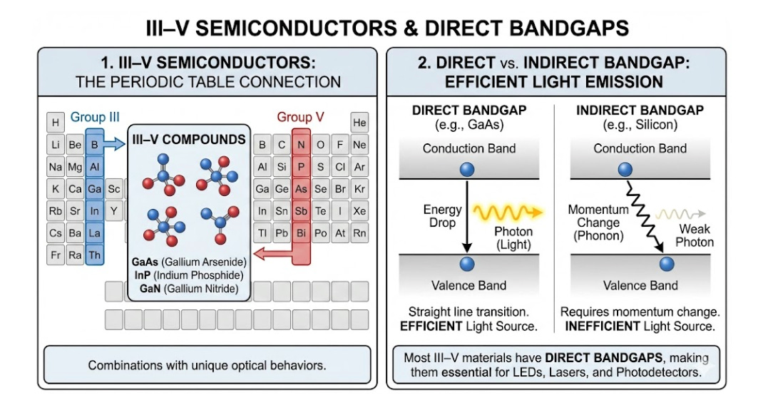
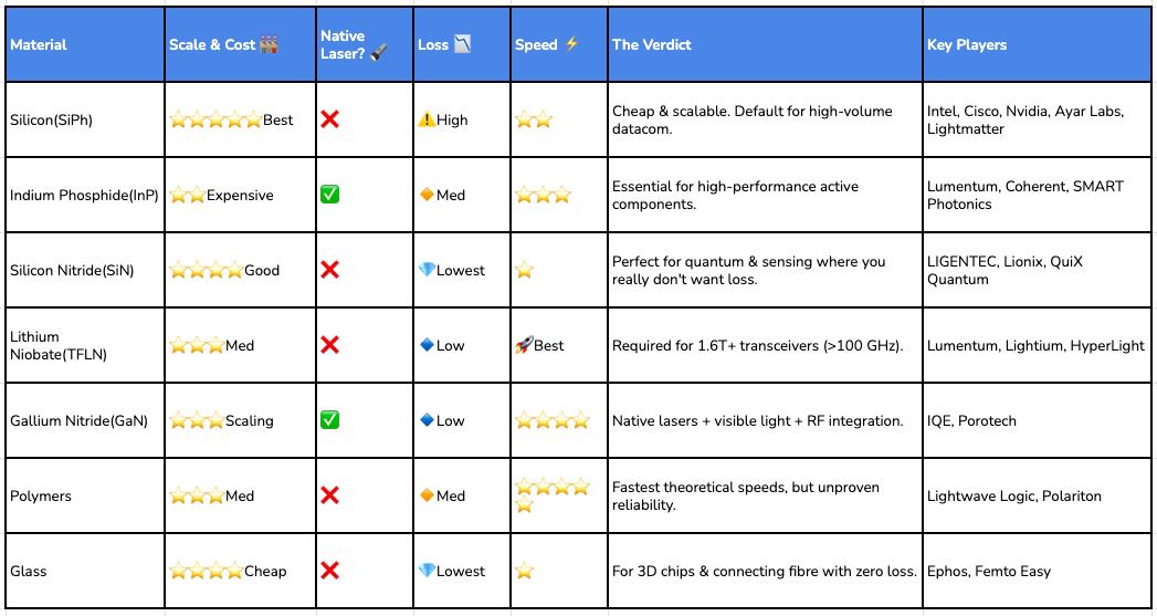
With James, I wanted to explore if gallium nitride (GaN) could become the material to make photonic chips. Other candidates include glass (Ephos), silicon nitride (LIGENTEC), indium phosphide (SMART Photonics), and thin-film lithium niobate (Lightium).
The timing of this conversation matters because James argues two shifts could erode the assumptions that locked the industry into silicon:
the rise of short-reach data centre communications where fibre loss is negligible, and
advances in hollow-core fibre that remove wavelength constraints for longer distances.
What did I learn
The wavelength constraint is weakening. Silicon photonics succeeded because it operates at wavelengths around 1310nm and 1550nm that travel efficiently through conventional glass fibre. These became industry standard because glass absorbs minimal light at those points, critical for transoceanic signals. The entire ecosystem of lasers, detectors, and test equipment was built on this assumption. Inside data centres though, signals travel metres rather than kilometres, making fibre loss negligible and wavelength choice flexible. Avicena already exploits this with GaN microLED clusters at 425–430 nm, ignoring telecom wavelengths entirely. Hollow-core fibre extends that flexibility further by sending light through air rather than solid glass, removing the absorption constraints that locked the industry into narrow bands.
Gallium nitride (GaN) might be more than just a power semiconductor. Most people know it from laptop chargers and EV electronics where efficient high-voltage switching matters most. But those same properties make it compelling for photonics. GaN offers native gain, letting you build lasers directly on chip rather than bonding them separately like silicon requires. It has a real electro-optic effect for encoding data, avoiding lossy workarounds. And it stays transparent from UV to far infrared, covering wavelengths silicon cannot reach. The manufacturing base already exists at scale for LEDs and RF chips. If you were designing an ideal photonic material without legacy constraints, it would look remarkably like GaN.
No single material dominates every metric.
Indium phosphide (InP) generates light natively but manufacturing remains low volume and expensive.
Silicon nitride (SiN) offers ultra-low losses and tight bending for compact circuits but cannot produce lasers or fast modulators.
Glass (SiO₂ or glass-core substrates) provides exceptional fibre coupling and works at panel scale but large curvature radii make dense circuits impractical.
Thin-film lithium niobate (TFLN, LiNbO₃) excels at high-speed modulation but processing has been difficult.
Gallium nitride (GaN) combines native gain, broad wavelength transparency, and existing high-volume supply chains, though photonic process development remains early.
Interview
James, what up? For readers who might not be familiar with photonics, let’s set the stage. When we talk about silicon photonics, we’re talking about using light instead of electrons to move data around chips and between computers. The industry has largely settled on silicon as the material of choice. Why is that, and what’s the problem with it?
The reason silicon photonics is exciting is because silicon is processed at high volume. We know how to do it, and it can be done fairly cheaply. But it’s actually a really poor photonic material. We’ve just hammered it into working properly because of all the investment and infrastructure behind it.
When you say “poor photonic material,” what do you actually mean? What can’t silicon do that an ideal material would?
Silicon doesn’t have what’s called an electro-optic effect, which is the ability to change how light behaves by applying an electrical signal. That’s how you encode data onto light. Because silicon lacks this, engineers have had to use workarounds involving doping the material with other elements, which creates higher losses. We keep getting better with modulation speeds, but there’s an expectation it’s going to top out because of these fundamental material limitations.
And silicon is only transparent above about one micron wavelength, which is fine for telecoms and data comms, but if you want to do anything in the visible spectrum or really long wavelength stuff for sensing applications, that’s a problem.
So the industry picked silicon not because it was the best material for the job, but because we already had massive manufacturing infrastructure for it from the electronics industry?
Exactly. It’s cheap and we know how to manufacture it, so we’ve developed these little hacks to carry on using the processes we know and love. But it will reach a bottleneck sooner rather than later.
This brings us to compound semiconductors, materials like gallium nitride that combine multiple elements. Most people who’ve heard of gallium nitride associate it with electric vehicle chargers or LED lights. You’re suggesting it could be important for photonics too. Why?
To some extent, we have to admit this is a long shot. But let me talk you through why we’re taking it.
Gallium nitride is the second highest volume semiconductor in the world after silicon. It’s used for LEDs, lasers, RF, and power electronics. So we’re not talking about some exotic lab material. This is manufactured at serious scale already.
What makes it better than silicon for photonics specifically?
It has a very wide band gap and is transparent right down to the near-UV and pretty far into the infrared. You can get fast modulation through a real electro-optic effect, not the workarounds silicon requires. Critically, you can get gain, which means you can integrate lasers directly onto the chip rather than having to attach them separately. You can get detectors on it too. So in terms of raw capability, it’s a much more complete photonic platform.
If gallium nitride is so much better, why hasn’t the industry already switched to it?
The wavelengths are wrong.
Explain that. I don’t think I really understand why wavelengths matter so much?
When we send light through fibre optic cables, certain wavelengths travel better than others. The industry settled on what are called the O-band and C-band wavelengths because conventional glass fibre has low signal loss at those specific wavelengths. All our lasers, detectors, and equipment are built around that assumption. Gallium nitride works best at different wavelengths that don’t travel well through conventional fibre.
So it’s a chicken and egg problem. The infrastructure is built around silicon’s wavelengths, which locks out materials that might be better but operate at different wavelengths?
Exactly. But that assumption, that we’re locked into telecom wavelengths because of fibre properties, is starting to break down.
Classic. So, what’s changing?
Two things. First, short-distance communication. Inside data centres, the distances are short enough that fibre loss doesn’t matter much. If you’re only sending light a few metres between servers, you don’t need the wavelengths optimised for crossing oceans. There’s a lot happening at short reach where wavelength choice becomes flexible.
And hollow-core fibre. This is a new type of fibre that’s fundamentally different from conventional glass fibre. In conventional fibre, light travels through solid glass, which slows it down to about two-thirds the speed of light. Hollow-core fibre has an air channel running through the middle, and the light travels through that air rather than through glass. That means it travels at essentially the full speed of light, a 50% speed increase.
So it’s faster. But how does that help gallium nitride?
The speed is nice, but the bigger deal is that because the light is travelling through air instead of glass, the wavelength constraints disappear. Conventional fibre only works well at specific wavelengths because of how light interacts with glass. Air doesn’t have that limitation. So hollow-core fibre works across a much broader range of wavelengths, including the wavelengths where gallium nitride performs best. The reason GaN has been locked out of datacom is that its optimal wavelengths don’t travel well through conventional fibre. Hollow-core fibre removes that barrier.
Let me make sure I understand the thesis here. You’re saying the industry locked into silicon photonics because of wavelength constraints imposed by conventional fibre. But those constraints are weakening because of short-reach communications inside data centres and hollow-core fibre for longer distances. And if wavelength constraints weaken, gallium nitride becomes a viable alternative?
“Yep. And there’s a third element which I think is very under-exploited: RF and microwave photonics, where you use light to generate and process radio frequency signals. Gallium nitride is already used heavily for conventional RF electronics, so we know it’s a good material for dealing with the RF/electronics requirements, but we could use photonics to better generate and process these signals. And in these applications, the light never leaves the chip, so you don’t care what wavelength it operates at.”
Let’s talk about what you’re actually building. What is Wave Photonics doing to prove out this thesis?
We’re doing some very long-shot stuff, and there’s a lot of development that needs to happen. We’ve just announced a project with the Institute of Compound Semiconductors in Cardiff to develop a gallium nitride photonic process.
What does “develop a process” actually mean? For readers who aren’t familiar with semiconductor manufacturing, can you explain what you’re creating?
Sure. When you want to make chips, you need what’s called a PDK, a process design kit. Think of it as a recipe book combined with a parts catalogue. It tells designers exactly how to create each component, what the manufacturing constraints are, and how everything fits together. Without a PDK, you’re starting from scratch every time.
Normally, developing a PDK for a new material takes a team of engineers six months or more, and that’s just for the first version which probably won’t work perfectly. We’ve automated most of that process and can do it in about three weeks.
So your core technology isn’t about gallium nitride specifically. It’s about being able to rapidly develop these recipe books for any new photonic material?
Exactly. The team in Cardiff are experts in processing gallium nitride. They know the manufacturing side. What we bring is the ability to quickly learn about a new material and fabrication process, test everything at high speed, and iterate rapidly. We have wafer-scale testing capability that’s designed to be very parallel and high throughput. We can get a wafer in and within a week have all the process data from all the components.
What will you have at the end of this project?
At the end of 12 months, we’ll have a passive process. That means components you don’t control electronically: waveguides that guide light around a chip, splitters that divide light beams, filters that select specific wavelengths. We’re not doing lasers or modulators yet. This is the foundation.
Why start with passive components rather than the more complex active ones?
Budget and time. But even just passive components are useful. You can use them for trapped atom and trapped ion quantum computing, which need specific wavelengths that silicon can’t provide. You can use them for chemical sensing in the infrared. So even this first version has real applications.
I want to push back on something. If gallium nitride is such a promising material, why isn’t everyone else pursuing this? What do your competitors think you’re missing?
We’re actually quite well hedged. We don’t care so much about the specific material. We can design for silicon, gallium nitride, silicon carbide, whatever. For us to develop on gallium nitride and start de-risking it is not a huge effort because of the automation we’ve built.
What’s been missed in the broader industry is this point about wavelength constraints loosening. It’s almost treated as an assumption that telecoms and data comms must happen in the O and C bands because that’s what works in fibre. Lasers are built around that, detectors are built around that, and everything else follows. That assumption was correct until short-reach communications and hollow-core fibre started changing things.
Most photonics startups I speak with are targeting AI infrastructure, trying to get designed into Nvidia or Broadcom products. Are you going after that market?
Almost every photonic startup except us has gone all in on that story. We do have some IP there from an acquisition. But our take is this: if you look at the big customers, Nvidia, Broadcom, they’re doing photonics themselves. To sell to them, you’ve got to do better than their internal teams, and these companies have trillion-dollar-plus market caps to throw at the problem.
Even the well-funded startups in this space, companies like Ayar Labs or Lightmatter, you don’t think they’ll succeed?
The technology and the teams are incredible, and in silicon I don’t think we’d be able to come close to competing with these companies, but even for them, my worry would be that the commercial path is genuinely hard when you’re competing with your customers’ internal efforts.
Fair beans, so what’s your alternative strategy?
Our thinking is that integrated photonics is useful for much more than just data comms. You don’t get quantum technology without integrated photonics. Anything to do with sensing in the visible or infrared. Gallium nitride deals well with radiation, so you can put it in space or near nuclear reactors. It’s transparent over a massive wavelength range for quantum computing applications.
We want to prove the material works across multiple applications before potentially going after the big AI infrastructure market. The level of money you need to be competitive in that space is $100 million plus. We want to do de-risking first.
And even if you did develop something dramatically better for AI infrastructure, is there demand for it?
Honestly, even if we developed something that’s a hundred-times increase in bandwidth density from today, I’m not sure there’s demand for that yet. The market might not be ready.
So to summarise your position: the big bet isn’t gallium nitride specifically, it’s a bet on the future shape of the photonics industry? Sort of a bet on heterogeneous photonics. Lots of different materials for lots of different applications.
The bet we’re going all in on is that photonics is not just going to be data comms and it’s not just going to be silicon. If we’re right on those two things, we’re in a very good position because we can move faster than anyone else I’m aware of on new materials and new processes.
Good man, James. Keep on fighting the good fight out there.
Debrief
So what did we think of that folks? Interesting, right? Well his thesis rests on two shifts. First, hollow-core fibre is genuinely impressive, but deployment is still early. Lumenisity, the leading company, was acquired by Microsoft in 2022 and has been relatively quiet since. The primary driver for adoption is latency for high-frequency trading, not wavelength flexibility. Whether datacom infrastructure actually transitions to hollow-core at scale remains an open question.
And second, short-reach communications inside data centres. This is on firmer footing imo. Distances are short enough that wavelength choice matters less. But silicon photonics vendors are not standing still. Intel, GlobalFoundries, and Tower Semiconductor all offer mature platforms with years of process optimisation and established supply chains.
James admits gallium nitride photonics is early. A passive-only process at six months is preliminary, with no lasers, modulators, or active components. The question is whether the underlying trend justifies exploration, not whether GaN displaces silicon next year.
Why the wavelength constraint argument matters beyond GaN
I thought his point on O-band and C-band lock-in, and the fact the entire industry is optimised for the 1310nm and 1550nm wavelengths was fascinating. The implications extend beyond gallium nitride. Equipment vendors, laser manufacturers, detector companies, and test firms all optimised for telecom wavelengths because that is where volume was. If wavelength choice becomes flexible, it reopens material and architecture decisions settled decades ago. Silicon photonics won partly on manufacturing cost and partly because it worked at the wavelengths that mattered. If that advantage weakens, silicon’s fundamental limitations as a photonic material become more exposed.
Second-order effects the market might be missing
Something I was thinking about after the interview on the dog walk was that if he is right, we might see a convergence between consumer electronics and data centre infrastructure. Gallium nitride is everywhere in consumer devices: LED backlights, fast chargers, RF front ends. If GaN photonics becomes viable, you have a material platform spanning consumer, automotive, communications, and computing. Higher volumes means getting prices down and more investment in wafers, tooling, etc to bring prices further down. Could we begin to see decreasing cost curves?
And quantum computing is another area where wavelength flexibility matters. Trapped ion and trapped atom systems operate at visible wavelengths silicon photonics cannot address. If the broader industry takes alternative wavelengths seriously for classical applications, the quantum ecosystem benefits from shared R&D investment. RF photonics is perhaps most underappreciated. Using light to process radio frequency signals offers advantages in bandwidth, electromagnetic interference immunity, and weight. Gallium nitride already dominates RF power amplifiers. Adding photonic capability creates integration possibilities that do not exist today.
The UK angle
The Institute of Compound Semiconductors in Cardiff is part of a broader cluster including IQE, the world’s largest independent epitaxy supplier, and Newport Wafer Fab. The strategic question for DSIT is whether compound semiconductor photonics represents a capability worth cultivating. The UK missed the silicon manufacturing wave, but photonics is earlier in its trajectory and compound semiconductors play to existing UK strengths. Early investment in alternative material platforms could position the UK well for a transition larger players are not yet taking seriously. The risk is a long-shot bet on an uncertain timeline. The reward is strategic capability in photonic materials that the US and Asia optimised away from when they bet on silicon. We would still have to invest substantially and move fast because it’s not like Asia and the US don’t see the photonics wave.
Speculative opportunities
Hybrid integration platforms combining the best material for each function become more valuable. You might use indium phosphide for light generation, gallium nitride for modulation at visible wavelengths, and silicon for electronics. Companies that design across these boundaries will be well-positioned.
Test and measurement equipment for non-telecom wavelengths becomes a bottleneck. The industry has invested heavily in instrumentation for O-band and C-band. If visible and mid-IR wavelengths matter, someone needs to build the equivalent ecosystem.
Also, design software needs to evolve. Current photonic tools assume telecom wavelengths and silicon or InP properties. The EDA companies are expanding into photonics, but their tools reflect current assumptions. Startups with more flexible simulation capability could find openings.
Want more?
Brilliant deep dive on the wavelegnth constraint problem. The point about how hollow-core fiber could basically unlock material choices that were structurally impossible before is kinda underrated. If datacenter distances really do make wavelength flexibility viable, we're prolly gonna see alot more heterogeneous platforms where each layer uses the best material for its job rather than forcing everything thru silicon.